Wiring and pinout
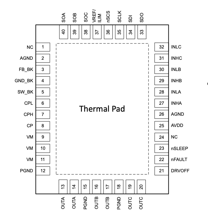
Connect SCLK to SPI clock, SDI to MOSI, SDO to MISO, and nSCS
to the configured active-low GPIO. nSLEEP controls device power state and
is required by the driver. nFAULT is an optional active-low input. Route
INHx and INLx according to the selected 3x or 6x PWM mode.
The diagram is an IC package pinout, not a board wiring diagram. Verify common
ground, logic levels, decoupling, charge-pump parts, current-sense routing,
motor-supply protection, thermal-pad connection, and layout against the
DRV8316 datasheet.
Warning
Power-stage wiring and configuration errors can damage the IC, motor, controller, or test equipment. The software documentation does not replace TI’s ratings, reference schematic, or layout guidance.